
Components
-
 Altera Nios II "soft-core" processor
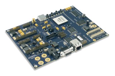
For the project, the Altera DE0-Nano board will be the most likely choice for payload projects. It features an Altera Cyclone IV FPGA and LEDs, dip switches, and debounce pushbutton switches for user interaction. For mobile applications, the board will need to be powered by a battery. For developing the code, the Altera DE2 board will be our board of choice. The board is already provided and wired in the digital lab on campus.
Altera Nios II "soft-core" processor
For the project, the Altera DE0-Nano board will be the most likely choice for payload projects. It features an Altera Cyclone IV FPGA and LEDs, dip switches, and debounce pushbutton switches for user interaction. For mobile applications, the board will need to be powered by a battery. For developing the code, the Altera DE2 board will be our board of choice. The board is already provided and wired in the digital lab on campus.
-
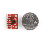 Triple-Axis Accelerometer
The sensor being used for measuring acceleration is the ADXL345 three-axis accelerometer. As the name suggests, it will receive and transmit acceleration data from all three axis. The data sent and received by the sensor will be done using the I2C peripheral included with the sensor. Two addresses are available for I2C communication. Two interrupt lines are available for use. These lines will allow for certain functions to be performed before resuming normal operations, such as reading acceleration data.
There are 57 available registers with 30 available to read and/or write. Some of these registers will be directly memory-mapped on the NIOS processor, such as the acceleration and interrupt registers. The unused or rarely used registers will have the ability to be accessed by setting up a memory-mapped lookup table of these addresses. This will allow other users to access these registers at a later date.
Triple-Axis Accelerometer
The sensor being used for measuring acceleration is the ADXL345 three-axis accelerometer. As the name suggests, it will receive and transmit acceleration data from all three axis. The data sent and received by the sensor will be done using the I2C peripheral included with the sensor. Two addresses are available for I2C communication. Two interrupt lines are available for use. These lines will allow for certain functions to be performed before resuming normal operations, such as reading acceleration data.
There are 57 available registers with 30 available to read and/or write. Some of these registers will be directly memory-mapped on the NIOS processor, such as the acceleration and interrupt registers. The unused or rarely used registers will have the ability to be accessed by setting up a memory-mapped lookup table of these addresses. This will allow other users to access these registers at a later date.
-
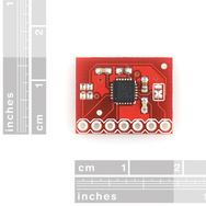 Triple-Axis Digital Output Gyro
The sensor which is being used for gyroscopic measurements is the ITG-3200 Triple-Axis Digital-Output Gyroscope. This sensor will provide Pitch, Roll, and Yaw data for real-time applications. The ITG-3200 features three 16-bit analog-to-digital converters (ADCs) for digitizing the gyro outputs, a user-selectable internal low-pass filter bandwidth, and a Fast-Mode I2C (400 kHz) interface. Additional features include an embedded temperature sensor and a 2% accurate internal oscillator.
The ITG-3200 triple-axis digital-output gyroscope includes three integrated 16-bit ADCs which provide simultaneous sampling of gyros while requiring no external multiplexer and optional external clock inputs of 32.768 kHz or 19.2 MHz to synchronize with system clock. There are 62 registers on the ITG-3200, 9 of which will be directly memory-mapped on the NIOS processor. The unused or rarely used registers will have the ability to be accessed by setting up a memory-mapped lookup table of these addresses. This will allow other users to access these registers at a later date.
Triple-Axis Digital Output Gyro
The sensor which is being used for gyroscopic measurements is the ITG-3200 Triple-Axis Digital-Output Gyroscope. This sensor will provide Pitch, Roll, and Yaw data for real-time applications. The ITG-3200 features three 16-bit analog-to-digital converters (ADCs) for digitizing the gyro outputs, a user-selectable internal low-pass filter bandwidth, and a Fast-Mode I2C (400 kHz) interface. Additional features include an embedded temperature sensor and a 2% accurate internal oscillator.
The ITG-3200 triple-axis digital-output gyroscope includes three integrated 16-bit ADCs which provide simultaneous sampling of gyros while requiring no external multiplexer and optional external clock inputs of 32.768 kHz or 19.2 MHz to synchronize with system clock. There are 62 registers on the ITG-3200, 9 of which will be directly memory-mapped on the NIOS processor. The unused or rarely used registers will have the ability to be accessed by setting up a memory-mapped lookup table of these addresses. This will allow other users to access these registers at a later date.
-
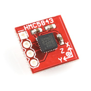 Triple-Axis Magnetometer
The HMC5843 is a tri-axis Magnetometer that is used for low field magnetic sensing that has a digital interface. This allows us to be able to use the HMC5843 to act as a compass or magnetometry. For our purposes we’ll be using it as a compass to be able to get a heading for the balloon. The way this works is the FPGA will input a clock to the HMC5843 as well as provide a data line that will act as an input and output to the FPGA and HMC5843. This is an I2C bus that works by the Master device, the FPGA, sending a start condition to the Slave device, the HMC5843. After receiving this start bit the Slave device waits for a device address to make sure the Master is talking with it. After confirming that the master is talking to it, it will wait for a signal to tell it to either wait to receive to start transmitting data.
This data will, as stated before, will be used to determine heading. Data is stored in 6 different registers, 2 for each axis. Once this data is ready a ready bit is flipped and will be pulled by the FPGA that’s waiting for this data. Once the FPGA reads that the ready bit is flipped it will send the send command to the HMC5843 and it will begin transition. Once it receives this data, the data will undergo calculations to convert it to a usable sum that will be displayed on a LCD.
Triple-Axis Magnetometer
The HMC5843 is a tri-axis Magnetometer that is used for low field magnetic sensing that has a digital interface. This allows us to be able to use the HMC5843 to act as a compass or magnetometry. For our purposes we’ll be using it as a compass to be able to get a heading for the balloon. The way this works is the FPGA will input a clock to the HMC5843 as well as provide a data line that will act as an input and output to the FPGA and HMC5843. This is an I2C bus that works by the Master device, the FPGA, sending a start condition to the Slave device, the HMC5843. After receiving this start bit the Slave device waits for a device address to make sure the Master is talking with it. After confirming that the master is talking to it, it will wait for a signal to tell it to either wait to receive to start transmitting data.
This data will, as stated before, will be used to determine heading. Data is stored in 6 different registers, 2 for each axis. Once this data is ready a ready bit is flipped and will be pulled by the FPGA that’s waiting for this data. Once the FPGA reads that the ready bit is flipped it will send the send command to the HMC5843 and it will begin transition. Once it receives this data, the data will undergo calculations to convert it to a usable sum that will be displayed on a LCD.
-
 Thermocouple Sensors
The Analog-to-Digital Converter (ADC converter) will be the main component responsible for refining signals from the attached thermocouple into a digital format. Once collected, the data will be sent to the FPGA via I2C or a similar peripheral where the FPGA will utilize software compensation to produce meaningful temperature data. ADC converters come packed a variety of features that will affect the final aspects and design of the thermocouple unit. Some features include filtering, programmable gain amplification, sampling rates, resolution and the number of thermocouple units that can be interfaced with the ADC converter.
In order to perform software compensation, the temperature at the inputs of the thermocouple unit to the ADC converter will have to be known. In order to produce a predicable temperature at this area, the ADC converter inputs will be heated by a piece of copper. After this a high resolution temperature sensor (such as a thermistor or RTD) will be utilized to record the temperature and transmit the data to the FPGA.
Thermocouple Sensors
The Analog-to-Digital Converter (ADC converter) will be the main component responsible for refining signals from the attached thermocouple into a digital format. Once collected, the data will be sent to the FPGA via I2C or a similar peripheral where the FPGA will utilize software compensation to produce meaningful temperature data. ADC converters come packed a variety of features that will affect the final aspects and design of the thermocouple unit. Some features include filtering, programmable gain amplification, sampling rates, resolution and the number of thermocouple units that can be interfaced with the ADC converter.
In order to perform software compensation, the temperature at the inputs of the thermocouple unit to the ADC converter will have to be known. In order to produce a predicable temperature at this area, the ADC converter inputs will be heated by a piece of copper. After this a high resolution temperature sensor (such as a thermistor or RTD) will be utilized to record the temperature and transmit the data to the FPGA.
This jQuery slider was created with the free EasyRotator software from DWUser.com.
Need a powerful Flash slideshow creator with built-in iPhone/iPad/Android support? EasyRotator is supported by the XML Flash Slideshow v4 Software.
OK
Need a powerful Flash slideshow creator with built-in iPhone/iPad/Android support? EasyRotator is supported by the XML Flash Slideshow v4 Software.
OK