
Key Accomplishments
Prototype Results
We have demonstrated a functional prototype which writes user data from an FPGA to a user-specified address on an SSD, and is able to correctly read the same values back from that address. Below are listed a few of the key results from the prototype roll-out.

During a write, which constitutes the main purpose of our design, the user data starts at the Application Layer (the external interface). The Transport Layer informs the storage device that it wants to write data, and upon receiving permission from the storage device it puts the user data on the line to the Link Layer. Inside the Link Layer, the data is formatted, scrambled and sent to the Physical Layer, at which point the scrambled data is serialized and sent to the storage device. More specifics on how and why these tasks are performed can be found later on this page.

The above SignalTap waveform shows the data signals internal to our design. When the couter values becomes available, the CRC (explained in the Frame Information Structure below) computation begins to obtain a value specific to the data provided by the user. At the same time, the user data is scrambled and sent on to the Physical Layer. You can see the same data word values appearing at the output of the Physical Layer after a time delay. During testing, we see the same values come back, verifying the correct operation of the read/write capabilities of our design.
Design: Data Flow Overview
Now that we've seen that our design works, we'll go through an overview of how it works.
We determined to divide the SATA controller into four primary layers: Application,
Transport, Link, and Physical. This structure enables the data flow to be more easily
followed and permits the separate subsystems to be developed and tested in parallel
without relying on the progress of any particular component. Each block will be implemented
as a separate component in VHDL, and combined in a top-down approach beginning with
the Application Layer, or External Interface.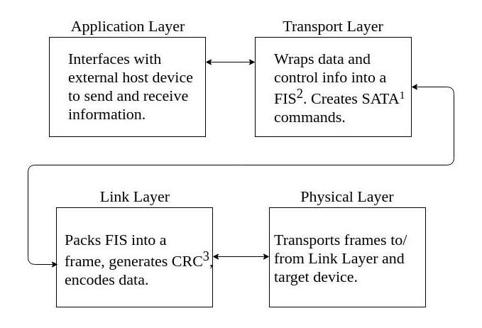
3. Cyclic Redundancy Checking
Application Layer: The External Interface

The first step in the data path is the Application Layer, which is where user data is collected from the host (aka the user). This will represent the External Interface in this project, which is depicted in a block diagram above. This interface will be used to connect the memory system to a device such as the hyperspectral camera in the Resonon UAV project. It has been designed to be a dual-port memory, which means there are separate address and data signals for reading and writing.
The abstracted, modular interface we provide enables the user to view our device as a simple dual-port memory sink without knowledge about the complex protocol that is making the data storage possible.
The data path for a write flows from the Application Layer to the Transport Layer, Link Layer, and finally Physical Layer before moving off the FPGA and going to the storage device.
The Transport Layer includes a transmit (Tx) and receive (Rx) buffer to hold input and output data. In our design, we decided to have the buffer size defined as a generic value so the user can easily customize for their specific application. For a default value, the buffers were scaled by the maximum SATA data frame size, which consists of 2048 32-bit data words, known as "Dwords" in the specifications. Combining this with a 64 bit address gives a total frame size of 24.576 kB. The buffers were designed to hold up to four frames, to ensure a level of margin during device operation.
The project has several constraints that this interface was optimized towards. The primary concern is write bandwidth, this interface should be optimized so that it does not unnecessarily constrain the data speed below the physical limitations that will be faced farther along the data path. The SSD limits the maximum write speed to 500 MB/s under optimal conditions, so this interface should be able to meet or exceed that mark to prevent a bottleneck. This requirement can be met by optimizing the ratio between the input clock rate, and the input data width. The smallest data width that makes sense would be 32 bits, because that represents the minimum data size that can be transported or stored using the SATA protocol. However, this would require a input clock frequency close to the value that was identified during background research to be a rough maximum for the capabilities of the Altera Cyclone V FPGA that is required to be used for this design. An option we considered was to use a 64 bit data bus width, which would scale the clock speed by 1/2 while still maintaining the data rate; however, SATA defines several commands as an odd number of 32 bit words, so the most logical solution was to design for a 32 bit data bus width. Testing of our design illustrated that we were well within timing requirements, validating this design choice.
Frame Information Structure (FIS) and Frame Construction

Figure: Diagram of a Frame Information Structure (FIS) as defined by SATA 3.1 protocol.

Figure: Diagram of a frame assembled by the link layer, indicating where scrambling and encoding is performed on the data.
Acronym Key:
1. Start of Frame primitive
2. Frame Information Structure
3. Cyclic Redundancy Checking
4. End of Frame primitive
We've seen an overview of how the data flows through the system, so let's take a closer look at how that data is formatted. Information is passed from the memory buffer (see external interface description above) to the transceivers in the form of Frame Information Structures (FIS) defined by the SATA protocol. FIS are generated in the Transport Layer of the SATA controller, and consist of a type header and a corresponding payload. SATA defines three FIS types: Setup, Register, and Data.
Setup is used for initialization of the communication link. Initialization is discussed further below.
Information flows through the communication channel in both directions, and the Register type is generally used for FIS coming back such as during a read application. The register flags are the primary way that errors are reported in the communication system.
Data is the type used for reads and writes, where the payload portion of the frame information structure is the information that the system is designed to store. In the Resonon Hyperspectral Imager application, this would be the data from the camera.
The Transport layer packages the data and sends it to the Link layer for further processing.
The Link layer is responsible for packaging the frame information structure in a way
that enables the transceiver to send it to the memory device.
The first step in this process is to compute and append the Cyclic Redundancy Check,
CRC, which is used to determine if the data is the same each time it is accessed.
A Linear Feedback Shift Register (LFSR) is applied to both the FIS and the CRC to
create a pseudo-random bitstream, which reduces electromagnetic interference and also
prevents long runs of the same value to aid in clock synchronization.
The scrambled bit stream is wrapped in Start of Frame (SOF) and End of Frame (EOF)
primitives to tell the transceiver how big the package is, and then the entire item
is encoded with 8b/10b encoding consistent with IEEE standards before it is sent to
the transceivers for delivery to the storage device.
Initialization State Machine

Figure: Block diagram of the host initialization state machine complying with SATA 3.1 protocol and reflecting design choices.
Before the data frames can be sent, the two sides of the process need to perform a complex handshake to make sure they are on the same page. The initialization state machine dictates how the host (data producing component) and the device (data storing component) establish a communication channel. The device initialization state machine is part of the SSD and is already set up. The host initialization state machine must be implemented in the FPGA fabric to properly interface with the device state machine, which requires strict adherence to SATA 3.1 protocol.
Although the states are mandated by SATA, there are design alternatives in which states
are included in the final state machine. For our design, we had the option to exclude
the speed negotiation states; however, we decided to include them so we could operate
our device at the varying speeds permitted by the protocol, making our design compatible
with more memory storage devices.
A second design alternative presented in the initialization state machine is whether
or not the controller supports asynchronous signal recovery. Signal recovery refers
to how the controller responds to a loss of signal between the host and the device,
specifically how the Reset state can be reached when power has already been applied.
With asynchronous recovery, either the host or the device can start the initiation
process, while synchronous recovery relies exclusively on the host. In addition, asynchronous
recovery causes the self-looping states shown in the figure to the right to return
to Reset if a specified delay has passed, which increases the probability of success
during initialization.
Several factors were considered while determining whether we wanted to support asynchronous
signal recovery, the most prominent of which were the dangers of metastability (an
unknown state) due to not using a clock edge, and the improved recovery probability
due to the device being able to reset the communication channel. It was decided that
the second consideration was more relevant to our project, so we chose support asynchronous
signal recovery to make our controller connection more robust.
Transceivers
At this point in our data path discussion, data has been passed down from the user's Application layer all the way to the Physical layer, being wrapped, scrambled and encoded along the way. The final step remaining now is the transition from the low speed, highly parallel FPGA fabric onto the serial wires connected to the SSD. This is done through Altera's Transceiver IP. The transceivers are Altera's way of providing users access to high speed serial data lines as required by modern applications, like the SATA protocol.
The Cyclone V ST is the lowest cost FPGA family that Altera makes which still includes 6 Gbps Transceivers as required by the SATA protocol.
Correct configuration of Altera's Transceiver IP will allow the device to lock to the data signal from the SSD and transmit serial data to and from the memory device. It also handles encoding the data into 8B/10B format.

Cyclone V Transceiver Configuration Options.
TX: Transmit
RX: Receive
PLL: Phase Locked Loop
PIPE/PCIE: Hard IP, not utilized
PCS: Physical Coding Sublayer
PMA: Physical Medium Attachment